
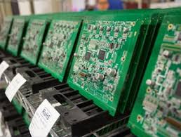
Solder Shorts During PCB Assembly
PCBs are a complex array of wires, traces, pads and terminals. The solder that connects these components is a critical link, and any problems with it will almost certainly limit the performance and reliability of the finished product and can even lead to a deadly short circuit. Solder bridges are one such issue; they can form between the conductive elements on a PCB, allowing current to flow where it shouldn’t. This article takes a look at some measures that are taken to prevent solder shorts during PCB assembly and ensure the quality of the finished product.
The first step in preventing solder shorts is to make sure the board has a layer of solder resist. This is typically a polymer that is silkscreened onto the top side of the board and then cured with heat, creating a barrier between the metal surfaces and the underlying copper. The most common material used is epoxy, which has the added benefit of being easy to work with and providing good electrical insulation.
Another important feature of a pcb printed circuit board assembly is the pad design. Pads that are too close together or too small can create solder shorting problems, as liquid solder is able to flow between them and cause a short-circuit. This can be avoided by using a larger pad size or a pad shape that offers good electrical isolation. Pad spacing rules must also be followed.
Preventing Solder Shorts During PCB Assembly
Solder shorts can also be caused by poor wetting, where the molten solder fails to properly adhere to the surfaces it is soldered to. This can be reduced by using high-quality solder and flux, cleaning the surface thoroughly before soldering, and adjusting the soldering temperature and duration to match the solder and material specifications.
Other potential causes of solder shorts include excessive solder paste, incorrect stencil alignment, and contamination from residues or other contaminants. These issues can lead to a lack of sufficient preheat temperature, which means the solder paste doesn’t liquefy and spread correctly during reflow. Insufficient preheat temperatures also increase the risk of pad bridging, where solder bridges between adjacent pads.
Component placement follows solder paste application, where automated pick-and-place machines accurately position the electronic components onto the PCB. These machines use computer-controlled mechanisms to pick components from reels or trays and place them onto the solder paste-covered pads with high precision and speed. Advanced pick-and-place machines can handle a wide range of component sizes and shapes, ensuring optimal placement accuracy.
Another potential problem is tombstoning, where the melted solder wicks up the leads of through-hole components instead of down. This can result in an incomplete solder joint and is a significant concern, especially as lead pitches continue to decrease. This can be prevented by using balanced pad designs, ensuring the proper hole-size-to-lead ratio, and by using good wave separation techniques.
Finally, excess heat can damage sensitive components, which can lead to a variety of malfunctions and failures. This can be avoided by utilizing heat sinks or dedicated copper planes to manage the thermal distribution of hot components, and by adhering to recommended temperatures and times for soldering.